Work in progress, November 2026. This page tells the design in the order you would build it and learn it: a transistor, a gate, a memory cell, a bus, an arithmetic unit, a control unit, an instruction set, an assembler, a compiler, a program. That is the order of Nand to Tetris, of James Newman's Megaprocessor and of Charles Petzold's book Code, and this machine exists to be learnt the same way, with the difference that every level is made of parts you can hold and every bit has a light on it. The reference for every number here is the design document; this page is the story, that page is the evidence. Everything marked simulated has been run in ngspice from a netlist generated by one script; nothing has yet been built.
The whole machine is one kind of part used one way. An NPN transistor with its emitter on ground, a resistor into its base and an LED and a resistor from the 5 V supply to its collector. Put about 3 V on the base resistor and the transistor conducts, the LED lights, and the collector falls to a tenth of a volt. Take the base to ground and the transistor is off, the LED is dark, and the collector rises to about 3 V. That is an inverter, and it is also the state indicator for free: the LED is the output.
Two things follow from the LED being in the load. The high level is about 2.9 V, not 5 V, because the LED and the resistor drop the rest. And the LED goes between the supply and the resistor, never between the collector and the signal, because a collector that must reach a tenth of a volt cannot do so through an LED. The first simulation of the first cell found this.
The family is called RTL, resistor-transistor logic, with diodes added for fan-in. The design document's electrical rules are the whole contract: supply, resistor values, how many loads a line may carry, and the three rules the simulation taught, that every transistor gets its own base resistor, that every line that can float gets a pull-up, and where the LED goes.
A NOR gate is the inverter with several inputs: a diode from each input to the base resistor, so that any input high turns the transistor on. An AND gate is a diode from the base node to each input with a pull-up resistor, so that any input low holds the node down. Put several AND nodes through OR diodes into one base and you have the gate the machine is built from: AND-OR-invert, one transistor, as many diodes as there are inputs. It computes "not (this and that, or those)", and because every stored bit in the machine is available in both polarities, that is enough for anything.
The one subtlety is level. Each AND diode lifts the node 0.6 V above the lowest input, and one OR diode drops it 0.6 V again, so with one diode of shift the base sits at 0.4 to 0.5 V in the off state, and two half-true terms together turn the gate on. A second series diode fixes it, as it did in DTL sixty years ago, and the margin is then 0.3 V off against 0.7 V on. Simulated, and the first version failed exactly this way.
A gate delay is about 0.3 µs, most of it the transistor coming out of saturation. Everything about the machine's speed follows from that number.
Two inverters, each driving the other, stay in whichever state they were left: a flip-flop, two transistors, two LEDs, one of which is lit. The machine stores every bit this way, and that is why it can run at any speed down to one phase every hundred seconds: nothing leaks, nothing needs refreshing.
Writing is done in two steps, lift then set. All the cells of a register share one emitter line through one transistor; turn that transistor off and the line floats, every cell falls to 0. Then a set transistor per cell, its base on the bus line and its emitter on the register's write line, pulls the cell to 1 wherever the bus is high. A read transistor per cell, its base on the cell and its emitter on the read line, pulls the bus line low wherever the cell is 0. Four transistors a bit for a register, three for a latch that does not need to drive the bus. Simulated: set in 0.03 µs, clear in 0.6 µs, read in 0.02 µs, and the clear needs its strobe to last between 0.5 and 1 µs, which sets the width of every clear pulse in the machine.
The set transistor can only write a 1, and the cell is transparent for as long as the write strobe lasts. That is why whoever drives the bus must keep driving it until the strobe has ended. The whole-machine simulation found this when the instruction register latched all ones.
There are seven registers of this kind: P, the program counter, and A, B and C for the programmer; IR holding the instruction; IN0 and IN1 holding the operands. P, A, B and C can read onto the bus; the other three feed the arithmetic unit and the decoder directly, in both polarities, for free.
Sixteen lines, each pulled up to 3.3 V by a resistor. Anyone may pull a line low; nobody may pull it high. So a register reads onto the bus by pulling low where it holds a 0, the constants 0, 1, 2 and 3 are nothing but diodes from the lines to a select wire, and the host computer, which holds the 64K words of memory, drives a 0 by grounding a pin and a 1 by letting go. The bus is 3.3 V so that the host, a Raspberry Pi, never sees 5 V. Simulated with every load on every line: the high is 2.9 V, a read is valid in under a tenth of a microsecond, and a line recovers in 0.66 µs.
The lines that enable reading, writing and the arithmetic unit's drivers each carry up to sixteen transistors and tens of milliamps, so each has a 2N2222 driver, a pull-down to feed it and a gate to decide it: three transistors a line, 29 lines. Each also has a 1 kΩ pull-up, because a line left floating with sixteen transistors on it becomes a path from a high bus bit to a low one, through one transistor forwards and another in reverse. Simulated: with P at zero, the bus highs sagged to 1.9 V and a fetch lost a bit.
Sixteen identical slices. Each takes a bit of IN0, a bit of IN1 and the carry from the slice below, and offers five results onto its bus line: the sum, the AND, the OR, the exclusive OR, and the bit from the slice above for the right shifts. Which one reaches the bus is chosen by an enable line, so each result is a transistor whose base wants the complement of the result, and in four of the five cases that complement is already a node in the slice.
Twelve transistors a slice. Two make b', the second operand or its complement, so that subtraction is addition. Two make x, the exclusive OR of a and b', in both polarities. Two make the carry out, in both polarities, each as one gate: carry is the majority of a, b' and the carry in, and majority is its own complement, so the other polarity is the majority of the complements. One makes the complement of the sum from x and the carry. Five are the drivers. The carry ripples one gate delay a bit, 5.0 µs across sixteen, and that is the slowest thing in the machine. A four-bit lookahead does it in 1.7 µs for the same transistors, is simulated and working, and is deliberately not in the design, so that every slice is the same and the machine can be sixteen copies of one small board. It is first in the list of future extensions.
Four flags: zero, a sixteen-diode OR of the bus into one transistor; negative, bit 15; carry; and CIN, which holds the carry the next addition should start from. Carry and CIN are separate because an instruction reads the carry flag and writes it in the same cycle.
Simulated: every sum bit of ten test patterns against Python; a diode carry chain, drawn for this machine in 2017, shown twice over not to work in this logic family.
Thirteen phases make one instruction, and a ring counter of thirteen stages, one lit at a time, says which. Each stage is a master and a slave flip-flop so that the token moves exactly one place on each pair of strobes however long the strobes are. Fetch the instruction into IR; read P and add one; read the first operand, from a register, a constant or memory, into IN0; the second into IN1; set CIN and decide whether this instruction executes; write the result to a register or to memory, and the flags; and, if the instruction read its operand from where P points, add one to P again.
The clock is the first circuit in every electronics book, two transistors flashing alternately, with a knob for the rate. A third transistor turns its edge into a tick. A generator of four stages turns each tick into the four strobes, clear and set for the data cells and the ring's masters, then clear and set for the ring's slaves, and holds the set strobes until the host has answered. The host's answer is one wire, READY: raised when it has finished with the bus in this phase, dropped when it has seen the latch happen. A slow host simply stretches the phase; a tick that arrives while a phase is running is ignored. At the slow end the host supplies the ticks instead and the machine single-steps, one phase or one instruction at a time, which is the whole point of it. Simulated end to end, astable to ring, and the generator alone found three faults in itself when its outputs rather than its states were watched.
Decode is 52 transistors: which register or constant each field names, which operation, whether the condition holds. The condition is latched before the result is written, because a conditional jump can clear the very flag it jumped on, halfway through its own cycle. The simulation found that too.
The host is the other half of control, and the other half of the lesson. It is memory, it is the clock when the machine is stepped, and it watches every phase against a software model of the machine and stops at the first disagreement, saying which block to suspect. The host section of the design document has the pin map and the measured timings.
One word, sixteen bits, one format: a destination, a first source, a second source, an operation, and a condition. Sources and destination are three-bit fields naming P, A, B, C or the constants 0, 1, 2, 3, each with a bit that says "through memory": the register holds an address and the operand is the word there. So a load, a store, a jump, an indexed access and a compare are not instructions, they are addressing. Writing to P is a jump. Writing to a constant throws the result away and keeps the flags, which is a compare. Reading through P fetches the next word as an immediate operand and steps over it. Writing to address 0xFFFF calls the host, which is how a program prints.
The operations are AND, LSR, ADC, SBC, XOR, OR, ROR, ASR, and ADD and SUB which may be conditional on negative, zero or not zero. The rule for what went in was "everything that costs almost nothing", and most of it is a driver transistor per bit.
The emulator, emu/emu.c, is the definition. The machine is correct when it agrees with the emulator at every phase, and the host checks that it does.
The assembler writes instructions as A = B ADD *C, or lt0 P = 0 ADD 0 for a conditional jump, one line a word. Above it a very small Forth, only enough to give the assembler subroutines, a stack and names, provides the runtime that the compiler targets. A test suite of 247 cases runs every instruction through the emulator.
C, because a school should not have to learn a toy language to use a toy computer. The compiler is a port of chibicc, a small C compiler whose source is readable in an afternoon, with a new back end that emits the Forth layer. It compiles twelve test programs and the library; floating point, bitfields and structures passed by value are still to do. The library's putchar calls the host; a slow putchar written in C that draws glyphs into the display memory is a lesson in why early machines had video hardware.
The program the simulated machine runs is seven words: load 2 into A; add to it the word at address 2, into B; subtract, into C; exclusive-OR with 1 and store at address 3; compare; jump back on negative. It exercises a register write, a memory read, a memory write, a compare and a conditional jump, and the 887-transistor netlist does exactly what the emulator does with it, which took six design faults to achieve, all of them now rules in the design document. Simulated: an instruction takes 156 µs with the host waiting the same time in every phase, about 6 thousand a second, and twelve minutes of computer time for a millisecond of machine time.
Hello world is a C program, a call to the host and a 40 by 30 text screen on HDMI. Tetris will fit.
The same C program runs at four levels, and the levels are how the machine is taught and debugged. Compiled with gcc on the Pi it runs on the ARM and writes straight into the Blinking memory, which proves the memory map and the screen. Compiled for the Blinking CPU it runs on the emulator on the ARM, which proves the compiler and the program. Then it runs on the Blinking CPU with putchar as a call to the host, about a thousand characters a second. Then it runs on the Blinking CPU drawing every character itself by writing words into display memory, and that is the one the lights are for: the statement *(unsigned *)0xE000 = 'H' is the address appearing in a register, the letter appearing on the bus, and the H appearing on the screen. The four levels are three choices made outside the program, which compiler, where it runs and which putchar it links, and the design document has the table. Because anything that must be fast can run at the first two levels, the speed of the transistor machine is never a problem; it exists to be watched. A mode line drawn by the host above the program's screen names the level, the run state and the clock, and a key switches between them, so the whole lesson needs the machine, a monitor and a keyboard and nothing else. The last level is a ladder of its own: run free, one instruction a key, one phase a key, and at the bottom one phase with an oscilloscope on it, where the host draws a simulated panel of every LED from the same generated netlist as the real one and runs ngspice on the gates around any light you point at, so the carry ripple and the gate delay appear as voltages against time, beside the real panel showing the same phase.
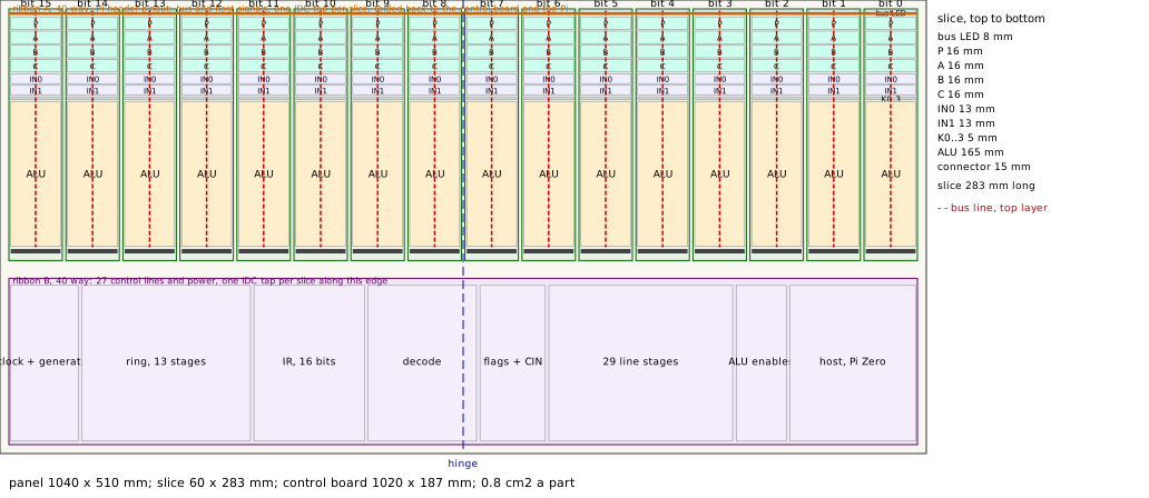
Sixteen slice boards and one control board. A slice is one bit of the machine: four register bits, the two operand latch bits, the arithmetic slice and the bus indicator, 35 transistors, 65 diodes, 20 LEDs, 81 resistors and one capacitor, about 400 solder joints. Two 40-way ribbon cables run along the row with a connector pressed on at every slice: one is the bus and the host signals, plugged straight onto the Pi's header, the other the 27 control lines from the control board; a six-pin link between neighbours carries the carry. The control board is the ring, the generator, the instruction register, decode, the flags, the 29 line drivers and the host interface, 327 transistors. The whole machine is 887 transistors, 1,816 diodes, 547 LEDs and 2,090 resistors, about 11,000 joints, on a panel a metre square. The LEDs are 3 mm, because five hundred 5 mm ones are too bright to look at, in a different colour for each kind of block, so that from across a room the ring, the bus, the registers and the arithmetic are told apart. Build order: one cell, one register, the clock and generator, the ring, one slice, sixteen slices, decode.
The boards are laid out to be read. The top copper layer carries signals and nothing else; power, ground and the strobes are underneath, the two things a schematic reader takes for granted. Every gate is placed the way its symbol is drawn, inputs on the left, LED above the collector, output on the right. The bus line is one straight track down each slice with every register cell beside it, the control lines are a labelled rail up one edge, the carry runs slice to slice along the row, and where two signals must cross the silkscreen draws the bridge. The sizes come from the generator's part counts: a slice is 60 by 296 mm, the panel about a metre wide and half a metre tall, with the layout rules in the design document. The same generator writes the KiCad netlists for the slice and the control board, so the boards and the simulation can never disagree. The host is a Raspberry Pi Zero 2 W, about £15, on the same 23 wires as the Pico alternative.
Designed, simulated or priced, and not in the machine, so that it gets built: the lookahead carry, faster strobes, per-phase host timing, higher display modes, the BBC Micro font as an optional pack, and a few more, in the design document.
Each section will grow a schematic drawn from the generator, a photograph when there is one, and the exercise a class would do at that level. The design conversations and the references behind every decision are on the conversations and references pages.